Fujitsu P23T-6 IPS
Specifications
| Brand: | Fujitsu |
|---|---|
| Model: | P23T-6 IPS |
| Size: | 23" |
| Resolution: | 1920x1080 |
| Panel type: | IPS |
| Max. refresh rate: | 60/75 Hz |
| Backlight type: | LED (white, edge) |
| LED driver: | OZ9967SN (o2micro) |
| TachistoMode: | wake-up |
| Price (approx.): | USD 460 |
| Monitor release date: | 2011-07 |
| This review's date: | 2012-12 |
Reaction time
Luminance curves have been measured for a slow counter-phase flicker stimulus switching between different gray levels. Measurements were taken at the very top of the screen with the photo diode PDA36A (Thorlabs) and signals have been recorded with the PC oscilloscope PicoScope 4224 (Pico Technology). The gain of the photo diode was set to 70dB, limiting the bandwidth to 12.5kHz.
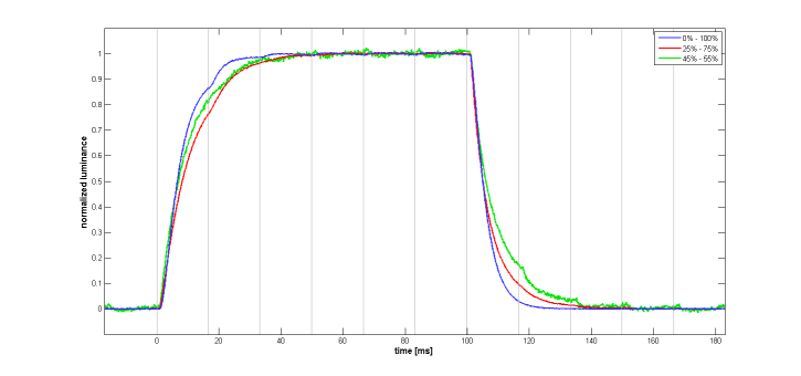
The measurements have been repeated with different monitor Contrast settings, but the results (not shown here) did not change much. Note that the monitor's Brightness defines the pulse width modulation ratio of the LED backlight and has to be set to 100% for these measurements so as to basically disable the PWM.
The curves shown in the figures have been scaled to a virtual step size of 1. Therefore, the noise level and signal modulation amplitude seemingly increase for smaller step sizes (especially evident for the green curve).
External LED backlight control
Under certain conditions this monitor is suitable for tachistoscope applications. The LED driver does not fully maintain the supply voltage level when the LED are switched off. However, the voltage level decreases relatively slowly over time and is quickly reestablished without major artifacts as soon as the backlight is switched on again. In applications where the induced errors cannot be tolerated, a brief wake-up pulse can be issued while "presenting" a black image, shortly before the actual stimulus image is going to be presented.
The measurements were taken with a photo diode PDA36A (Thorlabs) connected to a PC oscilloscope PicoScope 4224 (Pico Technology). The gain of the photo diode was set to 30 dB, limiting the bandwidth to 785 kHz.
LED switching characteristics
The measurements shown here were taken with an experimental scenario in mind where one stimulus (pulse) is presented per trial and a subject has to respond, inducing some variation of the inter-stimulus interval due to variable response times. The stimulus interval was randomly varied between 0.5s and 5s, uniformly distributed over a logarithmic time scale. Two different delays between the wake-up and stimulus pulse have been tested, 80ms and 800ms. These values were chosen with two scenarios in mind.
- The wake-up pulse is issued shortly before the stimulus. Because the wake-up pulse must not be visible to the observer, a black image has to be "presented" during the wake-up pulse. Thereafter, the software needs to switch to the stimulus image and the LCD has to settle to this new image, before the backlight can be finally switched on again for the stimulus pulse. The minimally required stimulus delay is mainly determined by the LCD reaction time (see Figure 1).
- The wake-up pulse is issued well before the stimulus presentation, for example, during the inter-trial pause. This implies a longer delay between the wake-up and the stimulus pulse.
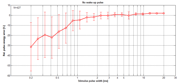
Figure 1 shows what happens if no wake-up pulse is used at all. Note that the error variability is basically owed to the inter-stimulus interval variability, which was rather huge as compared to the simulated response time variability, suggesting that this was pretty much a worst case scenario. On the other hand, the average of the inter-stimulus intervals was just around 1.5s (note that the inter-stimulus intervals were randomized on a log-scale). So it is pretty difficult to tell how big the errors would be when the inter-stimulus interval variability were smaller. Anyway, Figure 2 shows the errors when applying wake-up pulses, and these errors are not only smaller but also show far less variability as compared to the no-wake-up scenario.
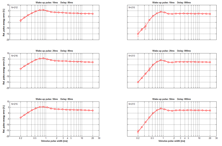
The relative errors shown in Figure 1 and 2 are given with respect to pulse energies which have been calculated as the product of the measured trigger pulse width and the steady-state luminance. Thus, the curves are free of errors which have been caused by inaccuracies in the trigger signal generation.
| rising (on) | falling (off) | |
|---|---|---|
| Delay [µs] | 7.8 (SD=±0.126) | 3.0 (SD=±0.047) |
| Slope [µs] | 14.7 (SD=±0.644) | 2.4 (SD=±0.114) |
Table 1: LED backlight switching times as measured from the rising and falling edges of the luminance curve when switching the backlight on and off. Shown are the average values with standard deviations. The delay is the time it takes for the luminance to change by 10% after the according trigger signal edge occurred. The slope is the time it takes for the luminance to rise from 10% to 90% (or fall from 90% to 10%, respectively).
Table 1 contains switching delays and speed values, averaged over all presentations which employed a 10ms wake-up pulse, an 80ms delay, and a trigger pulse longer than 1ms. For the rising edge, the delay was found to be considerable longer than for the falling edge. This caused the pulses to be systematically shorter than expected, namely by 3.0µs-7.8µs=-4.8µs. For a 200µs pulse, for example, this corresponds to a systematic relative error of -4.8/200=-2.4%. Moreover, there was a considerable difference between the rise and fall times. Given the numbers in Table 1 and assuming perfectly linear slopes, these errors would sum up to -5.5%. To some extent these effects possibly counteracted temperature effects in the LEDs, which are colder and therefore brighter at the beginning of the pulses and fall off as the pulses last.
Making the PWM signal available
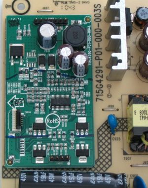
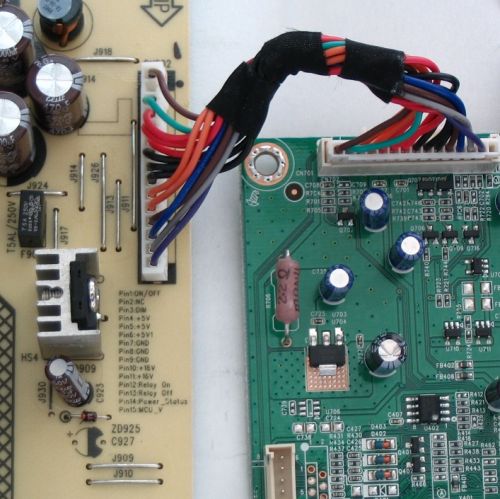
This monitor uses an OZ9967SN for driving the LED backlight. Making the PWM signal externally available is quite simple because this monitor has two printed circuit boards (PCBs), one for the monitor's control signals and another one for the power supply and the LED driver. Both are connected through a multi-wire connection which also carries the PWM signal for the LED driver. Signal ground is close by and, where needed, also +5V, all nicely documented right on the PCB. The logic level of the PWM signal at this point is 3.3V.
