Samsung SyncMaster S24A650
Specifications
| Brand: | Samsung |
|---|---|
| Model: | SyncMaster S24A650 |
| Size: | 24" |
| Resolution: | 1920x1080 |
| Panel type: | MVA |
| Max. refresh rate: | 60/75 Hz |
| Backlight type: | LED (white, edge) |
| LED driver: | BD9264EF |
| TachistoMode: | wake-up |
| Price (approx.): | USD 250 |
| Monitor release date: | 2011-11 |
| This review's date: | 2012-12 |
Models
There is an S and a D version. Apparently, the S version (i.e., S24A650S) comes with an USB hub and speakers whereas the D versions comes without.
Reaction time
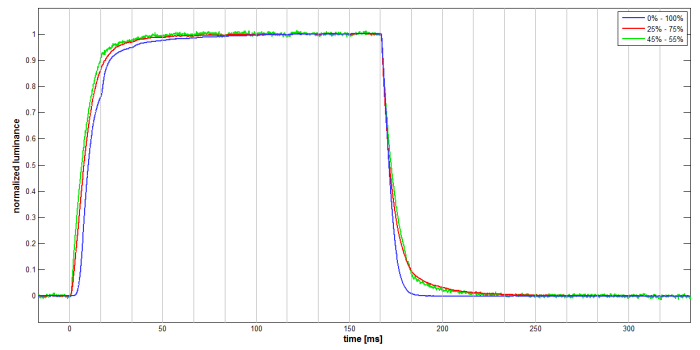
The luminance curves in Figure 1 were measured at a monitor's Contrast setting of 75%. The monitor also has a Response Time setting (overdrive) which was set to Faster, the 2nd level of three response time levels.
LED switching characteristics
The measurements shown here were taken with an experimental scenario in mind where one stimulus (pulse) is presented per trial and a subject has to respond, inducing some variation of the inter-stimulus interval due to variable response times. The stimulus interval was randomly varied between 0.5 s and 5 s, uniformly distributed over a logarithmic time scale. Two different delays between the wake-up and stimulus pulse have been tested, 80 ms and 800 ms. These values were chosen with two scenarios in mind.
- The wake-up pulse is issued shortly before the stimulus. Because the wake-up pulse must not be visible to the observer, a black image has to be "presented" during the wake-up pulse. Thereafter, the software needs to switch to the stimulus image and the LCD has to settle to this new image, before the backlight can be finally switched on again for the stimulus pulse. The minimally required stimulus delay is mainly determined by the LCD reaction time (see Figure 1).
- The wake-up pulse is issued well before the stimulus presentation, for example, during the inter-trial pause. This implies a longer delay between the wake-up and the stimulus pulse.
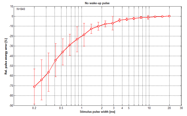
Figure 2 shows what happens if no wake-up pulse is used at all. Note that the error variability is basically owed to the inter-stimulus interval variability, which was rather huge as compared to the simulated response time variability, suggesting that this was pretty much a worst case scenario. On the other hand, the average of the inter-stimulus intervals was just around 1.5 s (note that the inter-stimulus intervals were randomized on a log-scale). So it is pretty difficult to tell how big the errors would be when the inter-stimulus interval variability were smaller. Anyway, Figure 3 shows the errors when applying wake-up pulses, and these errors are not only smaller but also show far less variability as compared to the no-wake-up scenario.
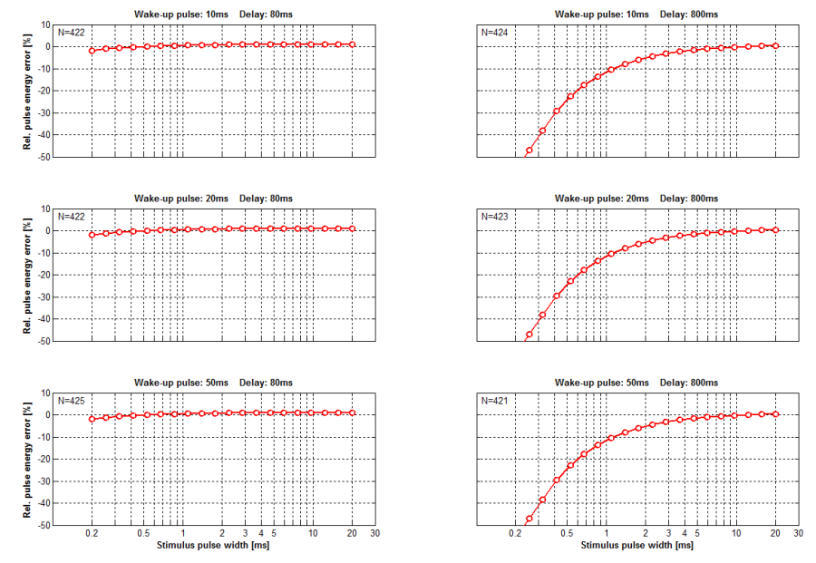
The relative errors shown in Figure 2 and Figure 3 are given with respect to pulse energies which have been calculated as the product of the measured trigger pulse width and the steady-state luminance. Thus, the curves are free of errors which have been caused by inaccuracies in the trigger signal generation.
| rising (on) | falling (off) | |
|---|---|---|
| Delay [µs] | 3.2 (SD=±0.051) | 2.6 (SD=±0.044) |
| Slope [µs] | 16.8 (SD=±0.777) | 2.6 (SD=±0.137) |
LED backlight switching times as measured from the rising and falling edges of the luminance curve when switching the backlight on and off. Shown are the average values with standard deviations. The delay is the time it takes for the luminance to change by 10% after the according trigger signal edge occurred. The slope is the time it takes for the luminance to rise from 10% to 90% (or fall from 90% to 10%, respectively).
The table contains switching delay and speed values, averaged over all presentations which employed a 10 ms wake-up pulse, an 80 ms delay, and a trigger pulse longer than 1 ms.
Making the PWM signal available
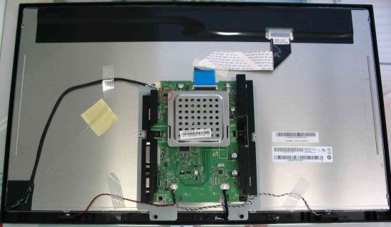
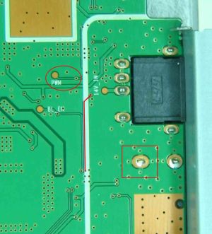
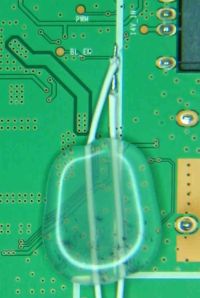
Making the PWM signal available externally is a bit tricky for this monitor because it has an external power supply and, thus, only one printed circuit board (PCB). Other monitors, which do have an internal power supply, often have two PCBs, one for the interface electronics and the other for the power supply and LED driver, making it necessary to route the PWM signal via easily accessible wires from one board to the other. Anyway, with this monitor it is a matter of disrupting a fine signal trace directly on the PCB and soldering wires to places where they are not meant to be. The trace in question is indicated by the red line in the close-up picture of the backside of the PCB. There is also a test point "PWM" (marked with a red circle in the same picture), which is basically the input of the LED driver. However, between this test point and the trace is a protective resistor (on the other side of the PCB) which should be used also for the modification; so we cannot use this "PWM" test point for soldering. The trace indicated by the red line is covered by the green solder mask and the white documentation print layer. These layers have to be removed down to the blank copper the trace is made of. This can be done by cautiously scratching it away with a small flat-head screwdriver. For easier soldering later on, it is important to leave the solder mask over adjacent copper traces and areas intact. Of course, also the very thin copper layer of the trace should stay intact. When this is done, the trace can be disrupted by cutting out a small piece. When soldering wires to the now open trace ends, be careful with mechanical forces; glue the wires onto the PCB afterwards so as to prevent them of ripping off the trace from the PCB.
The internal PWM signal complies to 5V logic.
